: Durable Elegance for Modern Applications")


High Quality Tellurium Nanomesh for Next Generation Electronics: A collaborative team led by researchers from City University of Hong Kong (CityU) recently invented an innovative method for synthesizing high-quality, semiconducting nanomesh at a lower temperature and production cost than conventional methods. The findings will help enable the large-scale production of nanomesh for next-generation electronics.
Nanomesh is a nano-scale material formed from a network of nanowires. For several decades, one-dimensional materials like nanowires made of crystalline inorganic materials have been widely explored as the main driver for emerging electronics, as they have features like mechanical flexibility, energy efficiency and optical transparency. However, the scalability, integrability and cost-effectiveness of nanowire semiconductors are insufficient, limiting their potential for large-area electronic and optoelectronic applications.
To overcome these shortcomings, a research team led by CityU scientists made a breakthrough, inventing a low-temperature vapour-phase growth method, which can achieve large-scale synthesis of semiconducting tellurium (Te) nanomesh for use in devices.
“The use of tellurium nanomesh in electronics holds great promise for meeting the emerging technological demands of today’s Internet of Things (IoT) applications. The progress made in this research marks a significant step towards the large-scale production of functional tellurium nanomesh, enabling potential applications that are not achievable through other means,” said Professor Johnny Ho Chung-yin, Associate Head and Professor in the Department of Materials Science and Engineering (MSE) at CityU, who led the study.
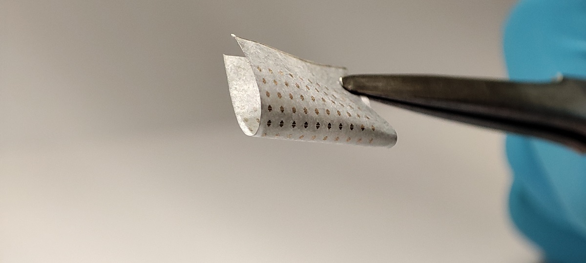
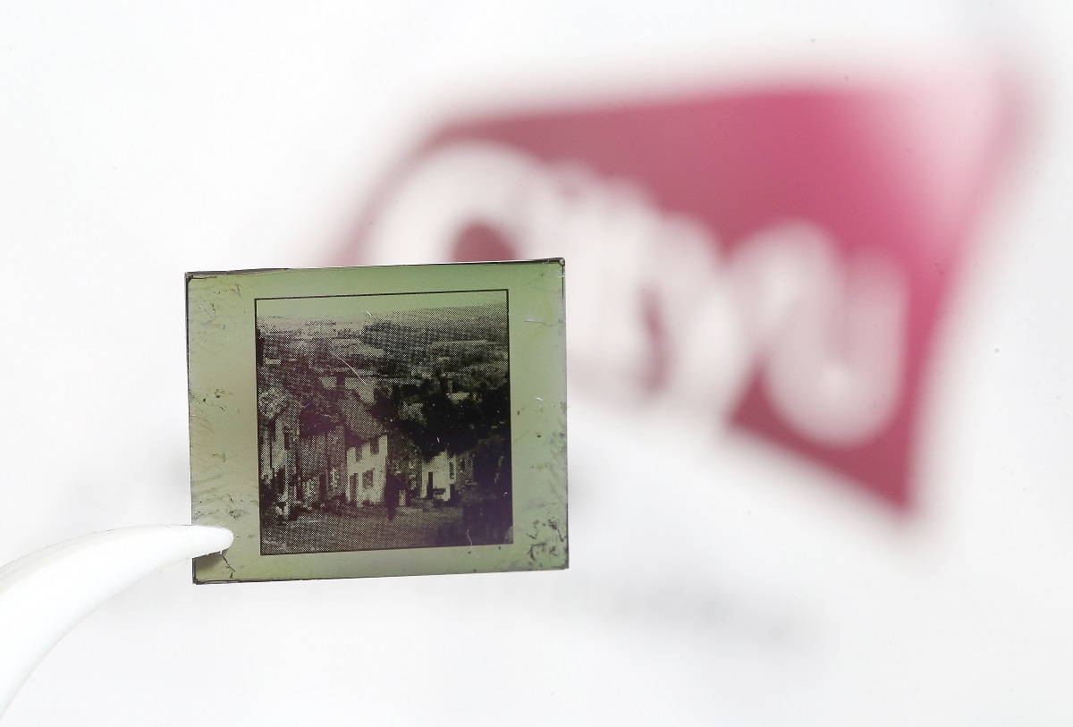
The newly developed method can produce high-quality tellurium nanomesh on various substrates, including silicon oxide, polymers (stretchable plastics), and even paper, in a scalable and cost-effective manner.
To initiate the growth process, tellurium source powders were first vaporised and carried to growth substrates, and then heated at 100 °C with a flow of argon gas. By employing the
principle of multi-scale van der Waals interactions of the materials in designing this novel synthesis method, the research team successfully created nanomeshes composed of self-assembled and self-welding tellurium nanowires laterally vapour-grown on arbitrary surfaces at the low temperature of 100 °C, which is impossible using conventional methods.
Since a much lower temperature than normal is required, and the nanomesh can be grown on various substrates, the production cost is lower. Also, the discovery of a self-welding process in the growth of tellurium nanomesh in the study is crucial for improving device performance and ensuring the mechanical robustness of flexible electronics.
Since a much lower temperature than normal is required, and the nanomesh can be grown on various substrates, the production cost is lower. Also, the discovery of a self-welding process in the growth of tellurium nanomesh in the study is crucial for improving device performance and ensuring the mechanical robustness of flexible electronics.
The experiments conducted by the team demonstrated multi-functional applications of tellurium nanomesh, including the capacity for micrometre-level patterning, the fabrication of high-mobility transistors, and the production of fast and sensitive infrared photodetectors (photoresponse time under 3 microseconds) on paper.
High Quality Tellurium Nanomesh for Next Generation Electronics: “All the obtained device metrics are on par with state-of-the-art devices, but can be produced at a lower cost. They are promising for meeting emerging technological demands,” said Professor Ho. “This latest development has improved the transport and photoelectric properties of nanomesh and resolved concerns about the compatibility between the target device substrate and the nanomesh growth process. As a result, devices can now be produced on a wide range of technologically functional surfaces in a scalable and cost-effective manner.”
The findings were published in the scientific journal Nature Communications under the title “Van der Waals nanomesh electronics on arbitrary surfaces”.
The first authors are Dr Meng You and Dr Li Xiaocui, postdocs in the MSE at CityU. The corresponding authors are Professor Ho, Dr Alex Wong Chun-yuen, Associate Dean (Outreach and Internationalisation) of the College of Science and Associate Professor of Chemistry at CityU, and Dr Wang Fei, Associate Professor of the Changchun Institute of Optics, Fine Mechanics and Physics at the Chinese Academy of Sciences. The collaborators include Professor Chen Fu-rong, from the MSE, and researchers from Kyushu University, the University of Electronic Science and Technology of China, Zhengzhou University, and Beijing University of Technology.
The research is supported by funding from the Research Grants Council in Hong Kong and CityU, as well as the transmission electron microscopy (TEM) facilities at the Time-Resolved Aberration-Corrected Environmental EM Unit and CityU.
High Quality Tellurium Nanomesh for Next Generation Electronics: Original Article
Flexible electronics breakthrough could lead to a revolution
Technique Uses Silver Nanowires to Create Flexible, Stretchable Nanowire Circuits
Tellurium nanoparticles achieve dielectric properties when exposed to sunlight


