An ultra-dark coating comprised of nearly invisible shag rug-like strands made of pure carbon is proving to be highly versatile for all types of spaceflight applications.
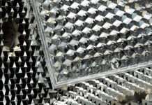
In the most recent application of the carbon-nanotube coating, optical engineer John Hagopian, a contractor at NASA’s Goddard Space Flight Center in Greenbelt, Maryland, and Goddard scientist Lucy Lim are growing an array of miniscule, button-shaped bumps of multi-walled nanotubes on a silicon wafer.
The dots, which measure only 100 microns in diameter—roughly the size of a human hair—would serve as the “ammunition” source for a mini-electron probe. This type of instrument analyzes the chemical properties of rocks and soil on airless bodies, like the Moon or an asteroid.
Although the probe is still early in its technology development, it’s showing promise, said Lim, who is using funding from NASA’s Planetary Instrument Concepts for the Advancement of Solar System Observations Program, better known as PICASSO, to advance the concept.
The Nanotech-Sized Electron Gun
Key to Lim’s instrument, of course, are the carbon nanotubes, which are excellent electron emitters. Discovered in 1991, these structures also exhibit an array of useful electronic, magnetic and mechanical properties.
To create these highly versatile structures, technicians place a silicon wafer or some other substrate inside a furnace. As the oven heats, they bathe the substrate with a carbon feedstock gas to produce the thin coating of nearly invisible hair-like structures.
For the electron emitter, Hagopian and Lim are using this technique to grow tiny, circular dots of carbon nanotubes in a grid pattern that Goddard’s detector branch fashioned using photolithography. Positioned above and below the lattice of dots are silicon wires or traces and a grid that produce two different voltages. These voltages create an electrical field that activates the release of electrons contained within the carbon-nanotube bumps or forests.
Read more: NASA eyes versatile carbon-nanotube technology for spaceflight applications
thumbnail courtesy of phys.org


